
-
Products
 Products
 -
Solution
 Solution
 -
Manufacture
 Manufacture
 -
Service
 Service
 -
News
 News
News -
About us
 About us
 -
Contact us
 Contact us


- Products
- Solution
- Manufacture
- Service
- News
- About us
- Contact us

Ultrafast lasers - Precision manufacturing
- Categories:切割下属子分类
- Time of issue:2022-10-14 13:22:32
- Views:0
Ultrafast Lasers - Precision Manufacturing
Ultrafast laser is a new generation of mainstream technology in the field of precision processing: ultrafast laser refers to a pulsed laser with a pulse width of output laser at the level of picoseconds (10-12 seconds) or less than that of picoseconds. Depending on the pulse width of output laser, Ultrafast lasers can be divided into picosecond lasers, femtosecond lasers, nanosecond lasers, etc. As an emerging material processing technology, ultrafast laser is one of the most important technical directions in the field of energy laser, and has significant advantages in processing.

Applied materials

Wafer

Glass

PCB/FPC

Ceramics

Membrane material

Characteristic material

Light source

UV

Infrared

Green light
CO2

Process method

Cutting

Draw a line

Slotting

Drilling

Lobes
Implicit
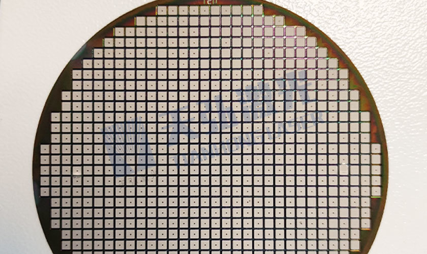
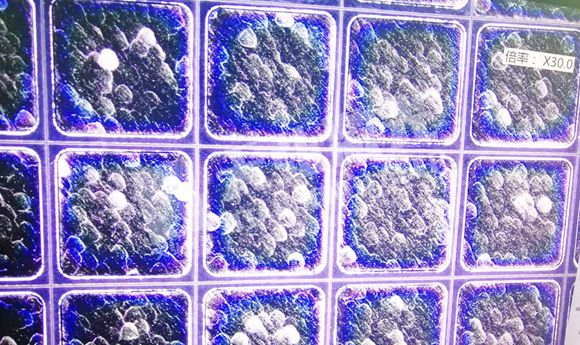
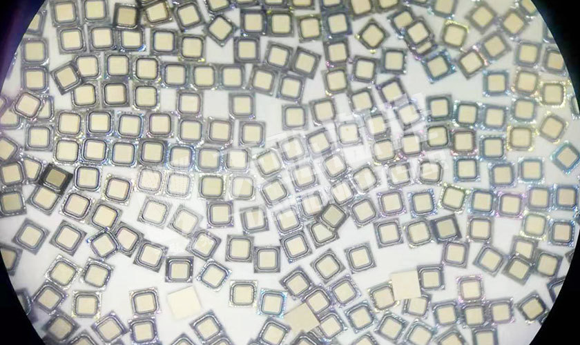
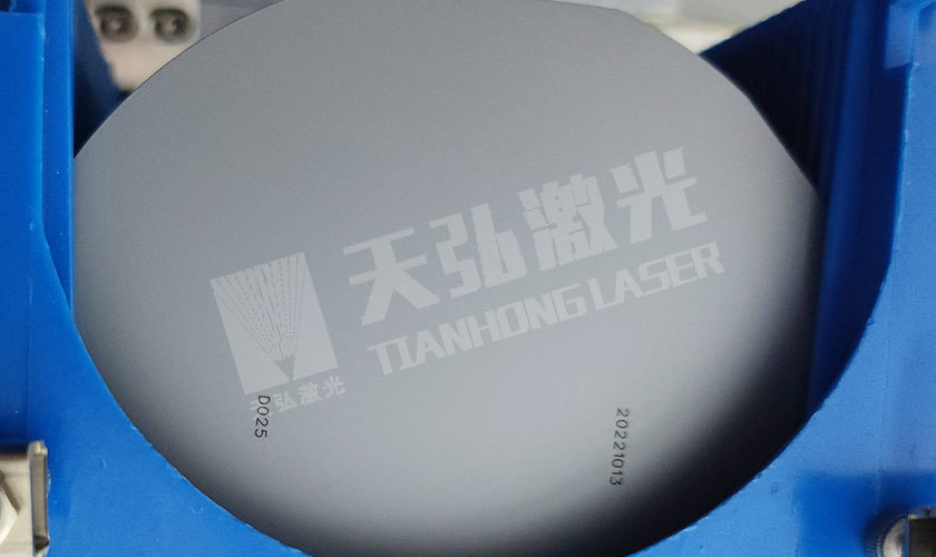
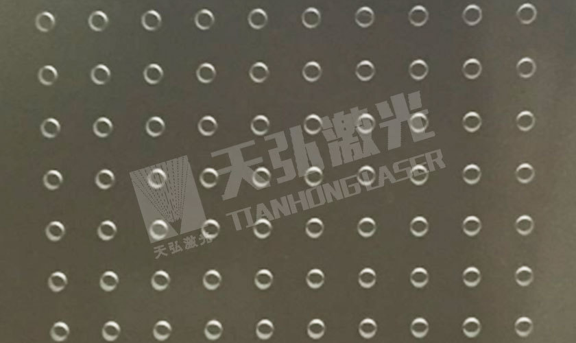
Typical Application - Semiconductor Wafer
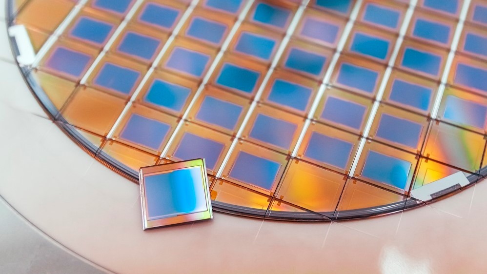
Semiconductor wafer
With the development of innovative applications such as automotive electronics and 5G, China's semiconductor chips are developing rapidly. The semiconductor industry chain mainly focuses on silicon wafer preparation, wafer manufacturing, packaging and testing. With the sharp increase in wafer integration, the wafer tends to become lighter and thinner. The traditional knife wheel cutting has certain limitations. It directly acts on the thinned wafer, which will cause greater thermal impact and cutting defects, such as Defects such as chipping, cracks, passivation, and metal layer lift-off, therefore, it is necessary to adopt a laser process with small processing heat impact, high processing accuracy and high efficiency. Celestica Laser has a comprehensive layout in the semiconductor industry, providing you with solutions and industry-specific machines covering the back-end process of semiconductor wafers, such as wafer bonding, wafer grooving, wafer cutting, wafer splitting, wafer edge cleaning, wafer A variety of laser application technologies such as wafer inspection and sorting, wafer marking, etc., meet the different needs of semiconductor companies.
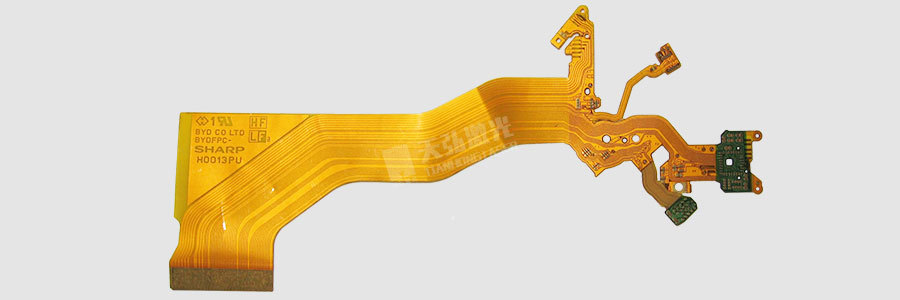
Typical Applications - Electronic Circuits
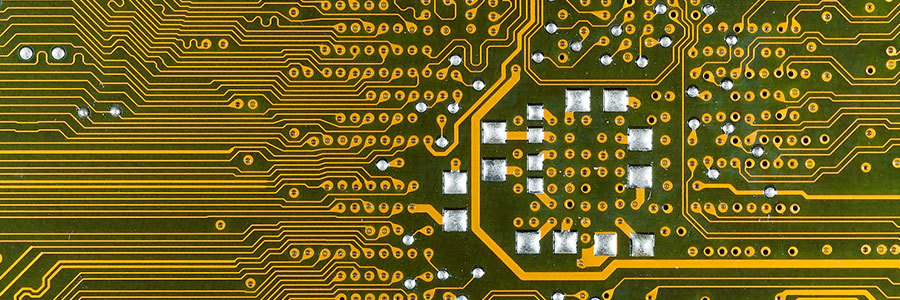
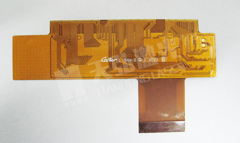
PCB
Keeping up with the development trend of intelligent manufacturing, Tianhong Laser is committed to providing industry intelligent solutions to reduce production costs and improve product quality and production efficiency for customers in the PCB industry.
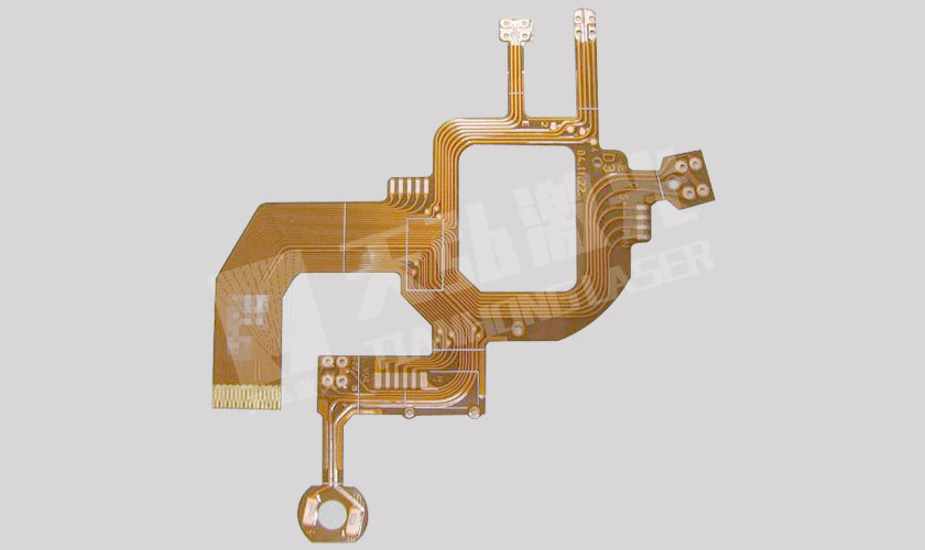
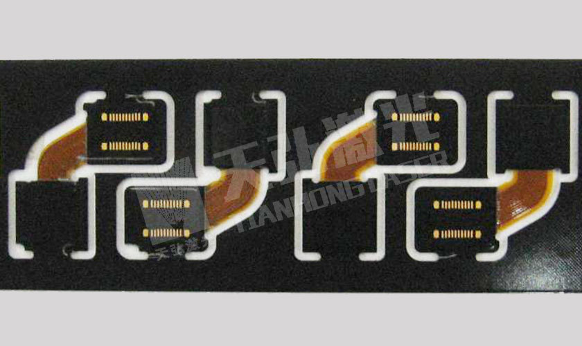
FPC
Tianhong Laser focuses on the application of FPC industry and creates professional solutions for the core process of the industry. With 21 years of technological accumulation, intelligent control, and meticulous craftsmanship, we can provide customers with more accurate and efficient industry solutions.
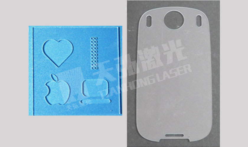
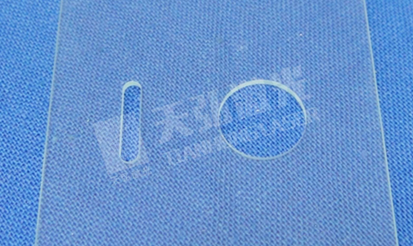
Typical Application - Display Touch

Display touch
The transfer of 3C products such as mobile phones from mobile terminals to smart terminals means that the functional requirements of products have increased, and mobile phone modules have become highly integrated and thinner. This trend brings new materials and high-precision requirements that make laser ultra-fast processing have significant advantages. In 3C and 5G-related industries, materials such as glass and ceramics are changing in the direction of "harder" and "more brittle". For the processing of brittle materials and flexible materials, laser micro-nano processing has replaced traditional processing methods to achieve laser cutting, drilling and so on. The processing technology of hole, welding and marking can achieve double improvement of processing efficiency and effect.
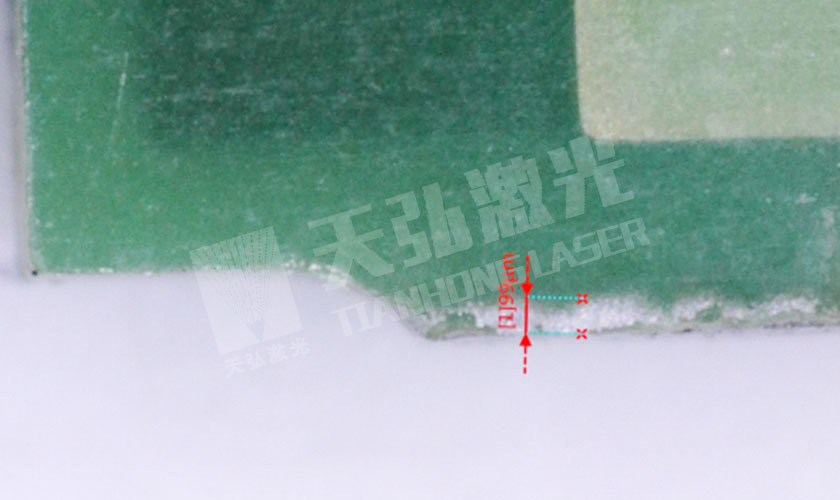
Fiber Laser - Metal Processing
Small heat affected zone
The ultrashort pulse generated by the ultrafast laser interacts with the material for a very short time, and will not bring thermal influence to the surrounding materials

High processing precision
Ultrafast laser processing has high precision, is not limited by the diffraction limit of light, and has high spatial resolution

No splash, no burr
There is no melting zone, no recasting layer, and no microcracks in the ultrafast laser processed structure

High degree of automation
It can be controlled by a computer, and it is convenient to process any complex shape

Non-contact processing
No tool wear, minimal heat-affected zone and deformation, capable of processing very small parts

Wide range of processing objects
There is no choice and restriction on the material, and any material can be finely processed

Industry Application
Semiconductor industry
Consumer electronics
Electronic circuits
Display touch
Medical biology
Photovoltaic energy
Precision machinery
Scientific research and Military
Advantage
SOFTWARE
MOTION CONTROL SYSTEM
OPTICAL SYSTEM


Cut样式表

Contact us
Company address
No. 66, Tonghe Road, Weiting Town, Suzhou Industrial Park

Website


Douyin